IWBNS-2006
4th International Workshop on Bulk Nitride Semiconductors
Oct. 17 - 22, 2006
Okubiwako Makino Prince Hotel, Makino, Shiga-pref., Japan
(near Kyoto)
TEL: 81-740-28-1111 (0740-28-1111 inside Japan) FAX: 81-740-28-1110 (0740-28-1110 inside Japan)
Following the success of three priors International Workshop on Bulk Nitride Semiconductors (IWBNS, in 2000, 2002, and 2004), on behalf of the Organizer Committee of the IWBNS-2006, we wish to extend a preliminary invitation to you in order for you to mark your calendar and plan to attend the IWBNS-IV. As the previous Workshop, this is "by invitation only" Workshop.
The Workshop will take place on October 17-22, 2006, during the week prior to the IWNS-06, in the Okubiwako Makino Prince Hotel, located at the Biwa Lake (Makino, Takashima City, Shiga Prefecture Japan), near Kyoto, Japan.
WORKSHOP TECHNICAL INFORMATION EXCHANGE
The Workshop will focus on the most recent advances and potential solutions to the remaining challenges of bulk group-III nitride crystal growth, and other substrates technologies such as chemical solution, fast growth, thick layers, polar and semi-polar substrates growth, characterization and properties (thermal, piezoelectric, [opto] electronics, etc.), lift-off techniques, homo-epitaxial growth, doping, surface preparation, device fabrication and characterization (on bulk substrates), modeling and theory.
All attendees are expected to present technical data on one or more of these topics above. Presentations will be limited to 10 minutes, followed by 10 minutes for questions. Lively discussion after technical presentations is strongly encouraged and will not be truncated. The atmosphere will be informal.
This Workshop is designed to exchange scientific information on problems and challenges in the science and technologies of fabrication of nitride-based bulk crystals and substrates with low concentrations of structural defects and unintentional impurities, and to avoid problems with hetero-epitaxial growth on substrates such as sapphire, silicon carbide, etc.
Seeded and unseeded bulk growth methods, low- and high-pressure, and fast/thick pseudo bulk epitaxial techniques will be addressed.
Growth and properties of undoped and intentionally doped homoepitaxial layers on bulk and thick heteroepitaxial substrates will be discussed. The growth and properties of device structures and the characterization of devices fabricated on these substrates are of high interest.
This Workshop will foster interaction between attendees from industry, government, and academia to address the current issues, research, and future potential of these technologies.
PROCEEDING OF WORKSHOP
The Proceedings will be published by the Journal of Crystal Growth and that information about the publication are described on the site:
http://authors.elsevier.com/JournalDetail.html?PubID=505670&Precis=DESC
(If you can't open this site by clicking the link, please copy & paste this web address to your address bar directly.)
WORKSHOP LOGISTICS
The Workshop will begin with a Welcoming Reception on Tuesday evening, October 17, in the Okubiwako Makimo Prince Hotel. Excursion will be provided on Thursday afternoon. Workshop sessions are scheduled for Wednesday, October 18, through the Wrap-up session scheduled for Sunday morning, October 22 a.m., after which the program officially concludes. The group will be returned to the Kyoto after the Wrap-up session by bus with taking a side trip on the way. All attendees are required to attend the entire Workshop to maximize information sharing and collaboration planning opportunities.
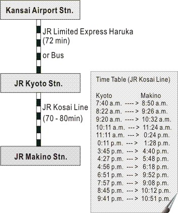
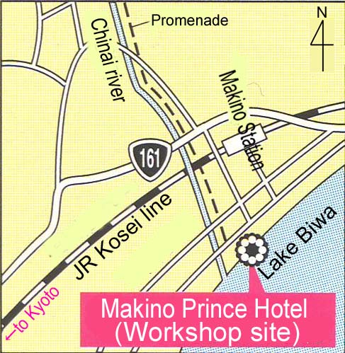
The Makino Prince Hotel on the Biwa lake is located at the north-northwest of the lake. Most of participants will arrive at Kansai International Airport (KIX). To get to the conference site, we have to go to Kyoto Station by JR(Japan Railway Company) Limited Express Haruka (100Km, 72 min, 3690 Yen), and go to Makino station by JR Kosai Line from Kyoto Station (67Km, approximately 80 min, 1100 Yen). It takes about 12 min to walk to the the Okubiwako Makino Prince Hotel from Makino station. Generally, you can take a ride in a bus, if you call to the Okubiwako Makino Prince Hotel (Tel: 0740-28-1111).
(Please see access map in this web page.)
All participants can choose an optional one-night stay plan in Kyoto (Oct. 16) for convenience. If you choose this plan, you will stay in Kyoto on Oct. 16 and go to Okubiwako Makino Prince Hotel (Workshop site) by bus on the morning of the 17th. Also, the sightseeing of Kyoto and its environs will be scheduled on the optional plan. Participants from oversea are strongly recommended to stay in Kyoto on Monday.
LOCAL ARRANGEMENT COMMITTEE FOR CONTACT
Prof. Tadashi Ohachi (Doshisha Univ.) is a chief of Local Arrangement Committee
Department of Electrical Engineering, Doshisha University
Kyotanabe-city, Kyoto, 610-0321, Japan.
Tel 0774-65-6329 (81-774-65-6329 from oversea)
Fax 0774-65-6811 (81-774-65-7811 from oversea)
e-mail tohachi@eml.doshisha.ac.jp
Handy phone: 090-3654-6999 (81-90-3654-6999 from oversea)